Snapdragon 805: GPU And The 4K Revolution
Adreno 420 GPU
The new GPU now has direct access to main memory, while the controller in Snapdragon 805 uses quality of service (QoS) to ensure each processing engine (GPU, CPU, ISP) receives the bandwidth and latency it requires for peak performance. Along with the bump in memory bandwidth, the texture and L2 caches are also larger. Adreno 420's rendering pipeline benefits from an enhanced early z-buffer test for faster depth rejection and improvements to the ROPs on the back-end.
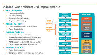
Qualcomm doesn’t provide any low-level details about its graphics architecture beyond those general enhancements. However, looking at the large increase in memory bandwidth and texture cache, I think it’s safe to assume that Adreno 420 wields more texture units. Qualcomm doesn’t mention if any changes were made to the design or quantity of shader units, or even GPU frequency, but based on our benchmark results, it’s likely that either one or both of these saw increases as well. According to Qualcomm, all of its improvements add up to 40%-higher performance and 20%-less power consumption than Snapdragon 800 running GFXBenchmark 2.7's T-Rex test at 1920x1080. We'll see if our benchmarks corroborate the company's claim, though we're forced to wait for a 805-based product to test the SoC's impact on battery life.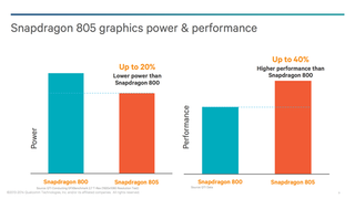
Adreno 420 does more than just raise the performance bar; it also improves rendering quality with support for OpenGL ES 3.1 and DirectX 11 feature level 11_2 (up from 9_3 in Adreno 3xx). It also adds support for geometry shaders and dynamic hardware tessellation, significantly reducing memory bandwidth requirements and power consumption, while simultaneously increasing scene detail. Rather than storing additional geometry mesh data in main memory and pulling it into the GPU, hardware tessellation generates the additional geometry detail programmatically on-chip without ever touching main memory.
The image below shows the visual advantage of tessellation, and according to Qualcomm, for “this simple hornet graphics scene, hardware tessellation delivers a bandwidth savings of ~360 MB/s, and a memory footprint savings of ~20 MB. For larger games, the savings on memory footprint could be in GBs.”

Another addition to Adreno 420 that can both reduce memory usage/bandwidth and improve visual quality is support for Adaptive Scalable Texture Compression (ASTC), the next-generation, lossy, block-based texture compression format introduced in OpenGL ES 3.0 (support is currently optional). ASTC offers developers more flexibility in choosing the appropriate texture size and quality than the ETC2 format used in the previous Adreno generation.

The 420 continues the Adreno tradition of using Qualcomm’s FlexRender technology to dynamically choose between two different rendering methods: immediate-mode rendering and tile-based deferred rendering (Adreno uses a different technique than Imagination Technologies). The goal of FlexRender is to select the most efficient rendering technique for a given workload.
Another efficiency feature is Dynamic Clock and Voltage Scaling (DCVS), which dynamically varies frequencies and voltages for each processing engine in the SoC. While this isn’t a new feature, the Adreno 420 GPU adds additional power levels for more granular control, reducing power usage.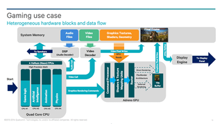
4K Video
Ultra-high-definition television (UHDTV), with a 4K resolution of 3840x2160 for the consumer version, is the latest video standard looking to replace high-definition television (HDTV), with its well-known 1920x1080 resolution. Living room adoption has been slow, however, due to the high cost of televisions and general lack of content. The situation is improving, though. Some 4K TVs sell for less than $1000, while Netflix and YouTube are currently streaming limited content in 4K. Amazon and Comcast are preparing to stream 4K video later this year, too.
For Qualcomm, big-screen TVs aren't driving 4K adoption. Rather, the company has its eye on the smaller, more mobile screens on our smartphones and tablets, as well as their 4K-capable cameras. With Snapdragon 805, Qualcomm hopes to push 4K harder. The new 805 is capable of concurrently driving its native panel at 4K (presumably at 60 Hz) and an external monitor at 4K/24 Hz.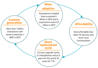
While Snapdragon 800/801 can encode/decode Ultra HD H.264 video in hardware, H.265 is handled in software. The 805 improves upon this by decoding 4K H.265 video in hardware. We'll have to wait for the Snapdragon 810 in 2015 for hardware-based encode, though. For now, the 805 can capture/encode Ultra HD video at 30 Hz and 1080p content at up to 120 Hz.
In the slide below, Qualcomm suggests up to a 75% power savings from the 805's hardware-based decode functionality.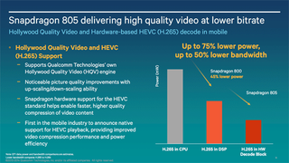
Snapdragon 805 also includes Qualcomm’s Hollywood Quality Video (HQV) engine, a technology purchased from Integrated Device Technology in 2011. The HQV engine is supposed to improve image quality by reducing noise and optimizing image formatting and conversion from various formats. There are also image enhancement algorithms for low-resolution images.
ISP
The Snapdragon 805 retains the dual ISP (Image Signal Processor) design used previously, but gets a performance boost. It’s now capable of processing 1.2 Gigapixel/s and image captures up to 55 MP across a combination of four camera inputs (up from two inputs in Snapdragon 800). The additional ISP inputs enable stereo and depth camera support.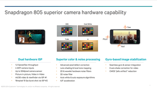
Also included in the 805 are gyro-based image stabilization, enhanced noise reduction, and auto-focus acceleration.