Wednesday, May 14, 2014

19 Ways to Do 3D Imaging

Perry West of Automated Vision Systems, Inc. publishes a nice whitepaper "Nineteen Ways to do 3-Dimensional Imaging" briefly discussing different approaches to get 3D images of various objects. Here is the summary table:

Tuesday, May 13, 2014

Pixart Expects Gesture and Heartbeat Sensors to Become its Main Growth Source in 2014

Digitimes: Pixart Imaging expects shipments of such gesture sensors to take off in 2H 2014, according to the company. In addition, Pixart has been developing heartbeat sensors for use in wearable devices and expects to begin shipments by the end of 2014, the company indicated. Gesture sensors and heartbeat sensors are expected to become the main source of revenue growth for Pixart.

A couple of months ago, Pixart has announced the design win of its gesture control sensor in Pantech smartphone. The new rumors say that Pixart sensor is used in the upcoming Amazon smartphone, although not telling if it's a regular image sensor or a gesture control one.

Monday, May 12, 2014

Image Sensor as Quantum Random Number Generator

Medium.com: A group of researchers from Geneva University, Switzerland, proposes to use image sensor as a high quality quantum random number generator, widely used in cryptography, security and other applications: "Quantum random number generation on a mobile phone" by Bruno Sanguinetti, Anthony Martin, Hugo Zbinden, Nicolas Gisin. The principle of their work in explained in the figure below. The random number quality has passed a number of tests for randommness.


Thanks to DM for the link!

Omnivision Announces Automotive HDR Sensor and Companion ISP

PR Newswire: OmniVision announces the automotive industry's BSI image sensor and a companion processing chip. The 1.3MP/60fps OV10640 delivers high sensitivity and HDR of up to 120 dB in highly compact automotive-grade packages, while the OV490 enables image and video processing for the next-generation ADAS systems.

"With the consumer predilection for advanced automotive features such as 360-degree surround view, lane departure warning and pedestrian detection, there is a tremendous demand among automobile manufacturers for imaging and processing solutions that deliver exceptionally clear, low-noise images and video," said Inayat Khajasha, senior product marketing manager for automotive products at OmniVision. "The announcement of the OV10640 and OV490 underscores OmniVision's position within the automotive industry as a trendsetter in developing sensors for next-generation ADAS applications."

The OV10640 is the first automotive OmniBSI image sensor, said to have the industry's highest sensitivity. The OV490 is a companion processor that enables simultaneous output of fully processed YUV or RGB data for display-based applications and RAW data for machine-vision downstream processing. The OV10640 and OV490 are now available for sampling, and are expected to complete AEC-Q100 Grade-2 qualification and enter volume production in Q4 2014.

ST "will soon offer products with 100’s of millions of pixels"

It came to my attention that STMicro image sensor web page has an interesting roadmap claim: "The current product portfolio spans a wide range of traditional image sensors from entry level VGA to 24 Mpixels and will soon offer products with 100’s of millions of pixels."

Sunday, May 11, 2014

Himax Reports CIS Sales Growth

Himax Q1 2014 earnings report updates on its image sensor business: "Our CMOS image sensors delivered a strong sales growth in Q1, up close to 30% sequentially. Our existing 2 and 5 megapixel CMOS image sensors are producing good sales from select international brands and Chinese white-box customers. However, as noted in the last earnings call, the current shipments comprise mainly of older generation products which are of higher costs. The sales of these products, given their rather significant amount by now, is the key reason why our overall corporate gross margin in the second quarter looks to stay flat or even go slightly down. Without it, our overall gross margin for the quarter would have continued to expand. Maintaining sales of such older generation products is necessary while we are going through design-in process with our customers to replace these products with new designs with much improved gross margins. The new generation products are expected to start shipments in the third quarter.

We expect our 8 megapixel sensors to start shipments later this year, which we believe will contribute to significant sales growth and better gross margin in the second half of the year. Additionally, following multi-year design efforts, we now have a competitive CMOS image sensor product line for automotive and surveillance markets, both large, lucrative and fast-growing markets. This is a market segment with a high barrier of entry where special know-how is required. Collectively, we expect the CMOS image sensor business to more than double in 2014.
"

Himax factsheet says that the company starts to mass produce optics for array cameras in Q2 2014:

Saturday, May 10, 2014

Polarization in Thermal Imaging

Optics.org: Polaris Sensor Technologies claims that polarized thermal imaging can offer so much more. David Chenault, the company president, says that their thermal camera with sensitivity to the light polarization, eTherm, is better at seeing at night, better at spotting a potential intruder behind a bush, or to see camouflaged targets. An extra advantage, is that it does not require temperature differences to create an image. "We can form the image from the material itself, from its texture and shape," says Chenault.

Sony Announces 12MP/14.5fps CCD and 8MP/30fps CMOS Sensor

Sony announces 8MP 1/4-inch IMX219PQ CMOS sensor based on 1.12um BSI pixels. The main improvement over its predecessor IMX111PQ is 2x speed, allowing 1080p60 video in 2x2 binning mode:


Sony also launches ICX834ALG (black-and-white) and ICX834AQG (color) 1-inch CCDs with 12.06M resolution. The new CCDs employ the 3.1um EXview HAD CCD II pixel, meaning that they offer a high sensitivity in NIR region. With 4 parallel outputs, the CCDs can achieve 14.5fps speed.

Friday, May 09, 2014

Pixart Q1 2014 Report

Pixart announces its Q1 2014 report. The revenue slightly decreased by 0.1% QoQ to NT$1,198.5M (39.8M USD). Due to favorable change in product mix and the depreciation of NTD, 2014Q1 gross margin was improved to 44.7% from 42.9% in Q4 2013. The operating margin increased to 7.3% from 5.9% in previous quarter. The net income for Q1 2014 was NT$91.8M (3.05M USD). The proportion of optical mouse sensors in the product mix grew to 90%:

Thursday, May 08, 2014

Omnivision Explains Image Ghosting Causes

Omnivision's patent application US20140117485 "Negatively charged layer to reduce image memory effect" by Howard Rhodes, Dajiang Yang, Gang Chen, Duli Mao, and Vincent Venezia talks about rarely mentioned but commonly observed ghost image effects: "The electrical signature of an image with high brightness levels that falls onto a complementary metal oxide semiconductor (CMOS) image sensor may remain embedded in subsequently read out electrical signatures of subsequently acquired images. The electrical signature of a previously sensed image remaining in the image sensor has been called a “ghost artifact” or a “memory effect.” This unwanted effect can be exacerbated by repeated exposure of static images, especially high intensity or bright images, to the image sensor. The retention of ghost images represents noise that obscures subsequently acquired images and reduces the signal to noise ratio and may cause blur if there is movement being imaged.

The memory effect problem has been found to be especially present in CMOS image sensors that have been fabricated using advanced fabrication technologies, particularly those employing measures to maximize metal interconnect density. For instance, those fabrication technologies employing so-called “borderless contacts” have been found to be associated with the root cause of this problem.
"

Omnivision explains: "The deposition of the contact etch stop layer is a fabrication technique that may be utilized when providing borderless contacts, which may be employed to increase metal interconnect density in pixel array."

Contact etch stop layer 322 is deposited over passivation layer 320, which is deposited over the pinning surface layers 313 included in example pixel array 302

"In one example, contact etch stop layer 322 may include a silicon nitride based dielectric including for example, silicon oxynitride, silicon carbide, or the like... The mobile charges in the PECVD silicon nitride and/or silicon oxynitride of contact etch stop layer 322 can be moved by electrical forces such as electrical fields placed across contact etch stop layer 322, which can cause unwanted effects in nearby semiconductor regions, such as photodiode regions 312 and/or the pixel circuitry included in the pixels of pixel array 302. For example, the source to drain resistance of a transistor included in the pixel circuitry included in the pixels of pixel array 302 may be affected by the mobile charge in the overlying PECVD silicon nitride of contact etch stop layer 322 by altering the depletion characteristics of an underlying lightly doped source or drain region.

Furthermore, it is noted that net positive charges can be induced directly in the PECVD silicon nitride and/or silicon oxynitride of contact etch stop layer 322 by exposure to visible light that may pass through contact etch stop layer 322, especially when photodiode regions 312 of pixel array 302 are illuminated with bright light when imaging. In particular, the energy associated with the phonon modes of the Si—Si and Si—H crystal structures may participate in the optical excitation of the electrical carriers. Consequently, memory effect is caused by the generation of positive charges in, for example, the SiON film of contact etch stop layer 322 that overlies the photodiode region 312 under the strong light illumination.
"

"To illustrate, FIG. 3A shows light 315 illuminating photodiode region 312, which therefore illuminates and passes through contact etch stop layer 322 as shown. This may occur when photodiode region is capturing an image. As a result of this illumination with light 315, positive charge 317 is induced in contact etch stop layer 322, which induces electrons 319 at the surface of the photodiode region 312 surface as shown.

FIG. 3B shows that after light 315 is no longer present and photodiode region 312 images a darker scene or is in a low light condition after having been illuminated with bright light 315 and after the image has been captured, the induced electrons 319 at the surface of the photodiode region 312 are injected into the photodiode region 312, causing the unwanted memory effect. In other words, when the pixel including photodiode region 312 images a darker scene, the induced electrons 319 at the surface of the photodiode region 312 that were a result of the previously captured image are injected into photodiode region 312, which generates localized dark current causing an unwanted “ghost image” of the previously captured image to appear as a memory effect in pixel array 302.
"

A nice explanation of the positive after-image. Indeed, many CMOS sensors have it positive. In some sensors the after-image is negative though - probably a different effect.

Wednesday, May 07, 2014

Microsoft Research Presents Visible Light Based Positioning System

Microsoft Research publishes "Epsilon: A Visible Light Based Positioning System" presentation by Liqun Li, Pan Hu, Chunyi Peng, Guobin (Jacky) Shen, and Feng Zhao proposing to use LED lighting to create an indoor GPS-like system:

Tuesday, May 06, 2014

Teledyne DALSA Opens Possibility Hub

Teledyne DALSA unveiles Possibility Hub - a content engine for sharing stories and knowledge about imaging technology and its ability to empower human achievement. Continued advances in digital image sensor technology and data processing are driving new and ever more ambitious applications for imaging technology. The Possibility Hub will spotlight these innovations not only in traditional industrial applications, but in the physical and health sciences, arts and entertainment, as well as oceanographic, geographic, and interplanetary exploration.

One of the articles on the Hub "Five CMOS Camera Developments to Watch in 2014" by Eric Fox. The developments are:
  • CMOS Sensors Will Go Big. Real Big. (in resolution and size)
  • CCD + CMOS: The Best of Both Worlds? (TDI implemented in CMOS)
  • Accelerating Speeds and Feeds
  • Better Low-Light Performance
  • More Will Be Happening On-Camera (HDR, ROI, various corrections)

Omnivision Announces 5MP 1.12um Pixel Purecel Sensor

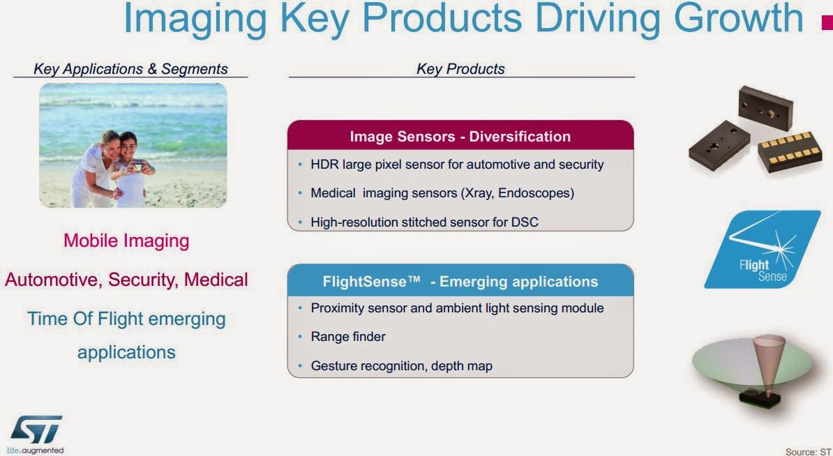
PR Newswire: OmniVision announces OV5670, the 5MP, 1/5-inch 1.12um PureCel image sensor for both front- and rear-facing cameras in smartphones and tablets. "The OV5670 is uniquely positioned in that it brings tremendous value and performance to camera applications on both sides of a mobile device. Its compact form factor and small optical format allow manufacturers to easily upgrade camera resolutions from 2-megapixel to 5-megapixel for main cameras in feature phones, and for front- and rear-facing cameras in smartphones and tablets," said Archie de Guzman, senior product marketing manager at OmniVision. "
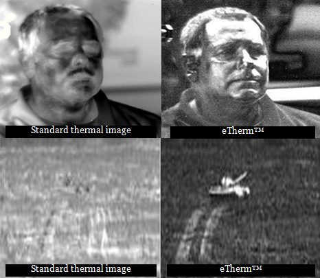
The popularity of mobile software applications focusing on video-conferencing has fueled consumer demand for higher-resolution front-facing camera solutions that also meet the space constraints of today's mobile devices. OV5670 provides an ideal solution."

The OV5670 PureCel image sensor capture full resolution 5MP images at 30fps, quad HD video at 30fps, cropped 1080p HD at 60fps, or 720p HD at 60fps. When recording 720p HD video with binning, the sensor achieves sensitivity and signal-to-noise ratio that is comparable to popular 1.75um pixel-based sensors. Additionally, the sensor's 1.12um pixel achieves similar full-well capacity as OmniVision's previous generation 1.4um pixel.

When the OV5670 is recording full resolution video, it uses approximately 35 percent less power than OmniVision's previous generation 5MP sensor. The sensor's ultra low power mode further reduces power consumption, thus minimizing battery drain. The OV5670 fits into 6 x 6 x 3.5 mm camera module. It is currently in volume production.

ON Semi Foundry Announces Image Sensor IP Blocks Availability

Business Wire: ON Semiconductor announces the availability of new qualified IP on its proprietary ONC18 180nm process. The new IP blocks were developed by various external vendors including Senseeker Engineering Inc., and range from small-pitch column-parallel ADC and cryogenic-compatible LVDS drivers to very-small footprint OTP memory:

Monday, May 05, 2014

Intellectual Ventures Wins Lawsuit Against Canon

Intellectual Ventures reports that the U.S. District Court for the District of Delaware rendered a verdict finding two Intellectual Ventures’ (IV) image sensor patents valid and infringed by digital camera products of Canon Inc. and Canon USA. Law360.com adds that "the jury held that Canon’s EOS 1DS Mark III, EOS 5D Mark II and Vixia Camcorders infringe at least one claim of U.S. Patent Number 6,023,081, which Canon failed to invalidate for obviousness."

The US 6,023,081 patent "Semiconductor image sensor" by Clifford Drowley, Jennifer Patterson, Shrinath Ramaswami, and Mark Swenson was originally filed by Motorola in 1997 and granted in 2000.

Sunday, May 04, 2014

Omnivision Proposes a Compact Way to Enhance DR in 4T Pixel

Omnivision's patent application US20140103189 "Compact In-Pixel High Dynamic Range Imaging" by Gang Chen, Duli Mao, Hsin-Chih Tai, and Howard Rhodes proposes quite a minor modification in 4T pixel which dynamically changes its conversion gain based on the signal level. The proposal is to add few Vth-adjust implants under the RST gate, so that various gate areas go to inversion mode depending on the floating diffusion voltage:

Saturday, May 03, 2014

DALSA CEO Retires

Teledyne DALSA announces that its CEO, Brian Doody, has decided to retire from the company to pursue other personal and family activities. Brian started with DALSA as its fourth employee in 1985 and rose through the ranks to become CEO in 2007.

Upon Brian's retirement, Rex Geveden, EVP Digital Imaging and Engineered Systems Segments, Teledyne Technologies Inc., will relocate to the Waterloo area and assume responsibility for the Teledyne DALSA business, as well as maintain his other segment responsibilities within Teledyne.

PMD ToF Camera in Direct Sunlight

PMD posted a Youtube video demoing its CamBoard pico XS in direct sunlight. "The tiny CamBoard pico XS can perform in direct sunlight -- no matter if the sun is shining directly into the lens or fully illuminating the scene. Due to the patented SBI circuitry (suppression of background illumination) pmd Time-of-Flight chips, and respectively pmd-based 3D camera systems, are very robust against ambient light."

Friday, May 02, 2014

Woodside Capital on Embedded Camera Market

Woodside Capital Partners publishes a 85-page-big report on embedded camera market "Embedded Camera Status: At The Edge of Depth", dated by Apr. 2014. The report essentially says that integration of the depth information into the cameras is the next big step in imaging: "The industry has acquired a thirst for depth detection in the cameras, and the generation of a point cloud of a scene, this has the potential to increase volumes shipped by nearly 2X by the latter part of this decade."

Few interesting graphs form the report:


The automotive camera section talks about the slow product launch cycle and market entry barriers:


Thanks to DM for the link!

ON Semi Closes Truesense Acquisition

On Semi announces the completion of its acquisition of Truesense Imaging. ON Semi paid approximately $95M in cash off its balance sheet, after adjustments for cash and working capital amounts, to purchase Truesense Imaging. Based on audited results, Truesense Imaging’s revenue for 2013 was approximately $79 million with gross and operating margins of approximately 44% and 23%, respectively.
Chris McNiffe, CEO and president of Truesense, has been retained by the ON Semiconductor team to help manage and grow our image sensor business. The Truesense product development and business teams will be incorporated in ON Semi’s Application Products Group (APG) as part of the company’s Image Sensor Business Unit, reporting to Vince Hopkin, VP of ON Semiconductor’s MDFI Division. The Truesense’s factory operations will report up through ON Semiconductor’s corporate manufacturing organization.

The former Truesense Imaging owner, Platinum Equity too announces the completion of the deal. "We are proud of this investment and of all the hard work that went into making it successful," said Platinum Equity’s Jason Leach, who led the initial Truesense acquisition from Kodak. "The business is fundamentally strong and is well positioned to succeed under new ownership."

Thursday, May 01, 2014

Mobile Photography Future

Embedded.com publishes an article "Mobile photography's developing image" by Michael McDonald, saying that resolution is not a differentiation factor anymore. Instead, the future camera phones will have computational photography features, such as HDR, super-resolution, 3D, imaging and more.